

Electron microscopy introduction

What does a brave Dutch woman physicist—who saved Jewish citizens during the Nazi occupation; a 19th-century British orphan who was appointed Elder Professor in Adelaide, Australia, at the age of 23; and a Czechia-born Viennese mathematician who revolutionized integral geometry—have in common? All of them: Lili Bleeker, William Bragg and Johann Radon laid the foundations of modern electron microscopy.
Continuing in the vein of self-study based blog posts, let’s understand electron based imaging together.
“I think I can safely say that nobody understands quantum mechanics” - Richard Feynman
A classic physics experiment of individual photons passing through a barrier with two parallel slits, causing each photon to create an “interference pattern with itself”, is striking in its implications about the wave-particle duality of light.
The incomplete timeline is as follows:
1801 - Thomas Young observes the interference pattern for light. No one questions the wave nature of light.
1887 - Heinrich Hertz observes a photoelectric effect experimentally. Negative electric charge is emitted from a UV irradiated zinc plate.
1905 - Albert Einstein provides a theoretical explanation of photoelectric effect with a hypothesis about light being composed of particles (photons).
1909 - G.I. Taylor shows the interference pattern can be obtained even with the faintest of light - approaching individual photons travelling through the double slit barrier “interfering with themselves”.
1961 - Claus Jönsson shows electrons create an interference pattern in a double slit experiment.
1989 - Akira Tonomura demonstrates that even when sending individual electrons an interference pattern emerges.
So… if electrons behave like light, can we use them for imaging?
Wavelengths, resolutions and reconstructions
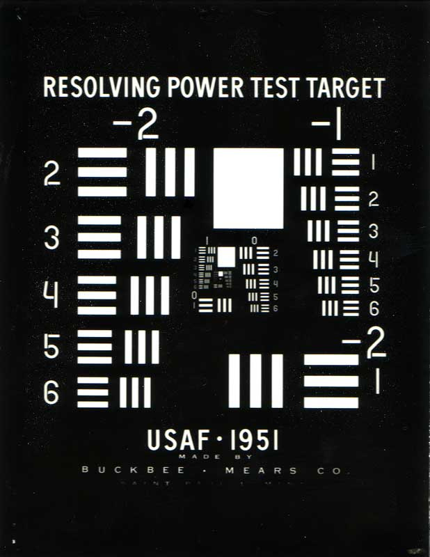
When photographing a test target with a monochromatic light, for aperture tending to 1.0, a theoretical image resolution approaches half of the light’s wavelength. For visible violet light of 380 nm that’s around 200 nm. Nanometer is one billionth of a metre.
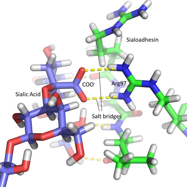
For atom level imaging, an Angstrom: Å, tenth of a nanometer is a useful unit. For example a salt bridge would typically be about 3Å long.
For X-ray crystallography a common wave choice is 1.54Å, produced by copper anodes in X-ray tubes. Resolution of structures at this level of precision involves taking pictures from many angles, utilising the periodicity of the crystal lattice, as well as incorporating physical knowledge to reconstruct raw X-ray diffraction patterns into a 3D structure that satisfies the conditions imposed by the 2D outputs.
Direct electron detectors
Theoretically the wavelength of electrons accelerated to 300keV energy is approximately 0.02Å. A beam of electrons is sent through a sample and focused with an electromagnetic lens whose focal length varies with the strength of electric current. One may date oneself if a TV cathode ray is a helpful analogy. These lenses operate in magnification modes of around 100.000x.
Prior to development of direct electron detectors, CCD sensors were used for electron microscopy imaging, by first directing scattered electrons through a solid state crystal scintillator which absorbed electrons and emitted photons for CCD to capture.
Currently machinery exists to capture the electron signal directly. They have two modes of operation: cumulative, where energies of multiple electrons interacting with a single pixel are added. And counting, where only the number of interactions is reported.
A modern direct electron detector like Apollo, will have the following specifications: 4096 x 4096 pixels. Each pixel is 8 micrometres wide, implying a 32mm x 32mm sensor. These pixels can report 12 bit (4096 values) deposited energy resolution. And are capable of a refresh rate of 60 frames per second. Pairing the sensor with an FPGA and utilising the time component allows the detector to quadruple its spatial resolution to 8K x 8K when in counting mode.
Phase contrast
CryoEM, which we’ll dive into next time, was recognised with a Nobel Prize in 2017. It builds upon an extraordinary feat of technical brilliance and theoretical insight: a phase contrast microscope. Recognised with a Nobel Prize in 1953 awarded to Fritz Zernike “for his demonstration of the phase contrast method, especially for his invention of the phase contrast microscope”. That microscope was manufactured by a factory founded by afore mentioned Lili Bleeker, a physicist and entrepreneur of enormous wartime bravery.
In light microscopy, waves passing through objects of slightly different refractive index, will undergo a phase shift. When refocused with a lens, aligned waves will strengthen (constructive interference) or when out of phase dampen (destructive interference).
Defocussing trick
For any given wavelength there will be lens and objective configurations that may extinguish the wave (see an informative video on Contrast Transfer Function). It’s therefore standard practice to capture images at various defocus ranges and to combine and resolve them in post processing.
Back to school: diffraction and Fourier transform
Both of these concepts were developed in the 1910s. Bragg’s diffraction in 1913 and Radon’s transform in 1917.
Diffraction
When a moving particle, photon or high speed electron, encounters a periodic grid and interacts with it, the angle at which it changes its course of flight is strictly determined by its wavelength, periodic spatial frequency of the grid (and an integer diffraction order). With certain a priori knowledge about protein chemistry, combined with a vast number of electrons at different defocus lengths it’s possible to reconstruct the distances between atoms that caused a particular electron scattering angle.
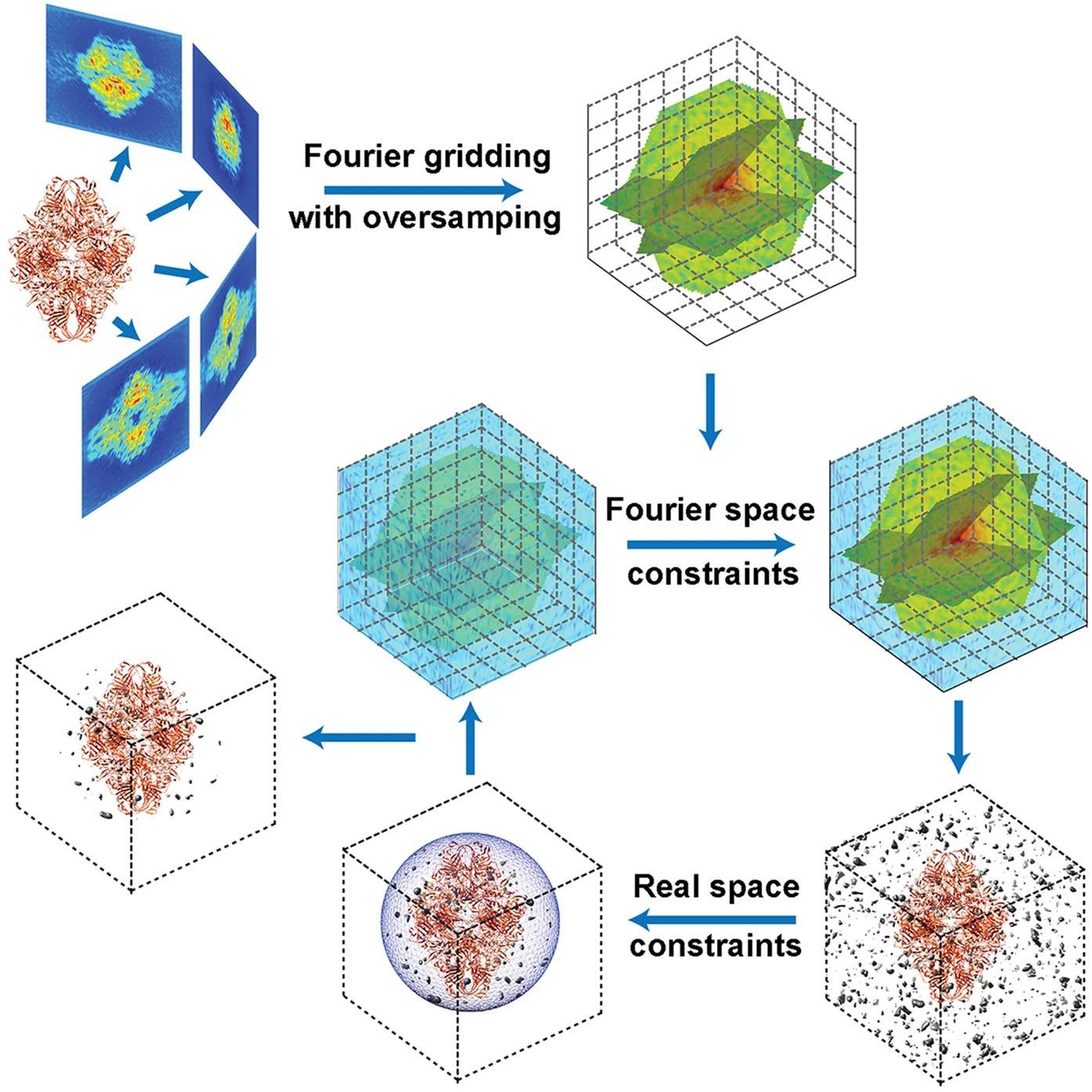
Radon transform based Fourier reconstruction
Operations in frequency (Fourier, reciprocal) space have always had an element of magic to them. Transforming signals or images into complex numbers with numerically delicate phases, multiplications with kernels and coming back into image space with numerically accurate convolution was an early computer science thrill.
For 3D imaging via 2D image capture we take things a step further: we reconstruct an actual 3D structure in frequency space. Imagine trying to guess a 3D pixel cube containing a protein. It can be proven that taking 2D projections (microscopy images) at various angles, computing their 2D Fourier transforms and placing them in a 3D frequency cube, when inverted back to pixel space will be equivalent to reconstructing the 3D pixel model of a protein.
The scale of it all
It’s important to appreciate the scale of post-processing required to complete such 3D imaging. To calibrate the direct electron detector based microscope on two known protein structures, a vast amount of data was collected.
Aldolase [PDB]: 8,682 movies, 1,824,301 particles. Achieving 2.24Å resolution
Apoferritin [PDB], 3,804 movies and 401,410 particles. Achieving 1.66Å resolution
Aldolase 3D structure from PDB.
References
Nobody understands quantum mechanics - a short YouTube clip of Richard Feynman.
Ruizhi Peng, Xiaofeng Fu, Joshua H. Mendez, Peter S. Randolph, Benjamin E. Bammes, Scott M. Stagg, Characterizing the resolution and throughput of the Apollo direct electron detector, Journal of Structural Biology: X, Volume 7,
2023.
Next time on atoms embeddings and forces
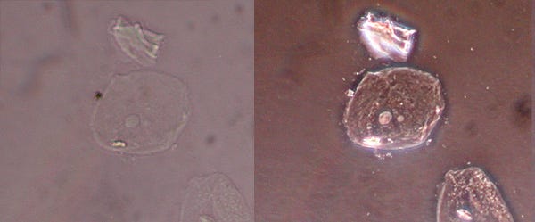
Cryogenic electron microscopy, a technique awarded the 2017 Nobel Prize in Chemistry to Jacques Dubochet, Joachim Franke and Richard Henderson, has accelerated scientific progress, by simplifying preparation and measurement of isolated protein samples compared to the previous imaging workhorse: X-ray crystallography. The crystallisation step - slow growth of a stable lattice of proteins - is replaced with “flash freezing” of randomly oriented proteins with liquid ethane at just above its melting point of -183C.
#atoms